- 您现在的位置:买卖IC网 > Sheet目录868 > LTM4604IV#PBF (Linear Technology)IC DC/DC UMODULE 4A 66-LGA
�� �
�
�LTM4604�
�APPLICATIONS� INFORMATION�
�Ratio� metric� modes� of� tracking� can� be� achieved� by� selecting�
�different� resistor� values� to� change� the� output� tracking� ratio.�
�The� master� output� must� be� greater� than� the� slave� output�
�for� the� tracking� to� work.� Linear� Technology� Tracker� Cad26�
�can� be� used� to� implement� different� tracking� scenarios.� The�
�Master� and� Slave� data� inputs� can� be� used� to� implement�
�the� correct� resistor� values� for� coincident� or� ratio� tracking.�
�The� master� and� slave� regulators� require� load� current� for�
�Parallel� Operation�
�The� LTM4604� device� is� an� inherently� current� mode� con-�
�trolled� device.� Parallel� modules� will� have� very� good� current�
�sharing.� This� will� balance� the� thermals� on� the� design.�
�Figure� 16� shows� a� schematic� of� the� parallel� design.� The�
�voltage� feedback� changes� with� the� variable� N� as� more�
�modules� are� paralleled.� The� equation:�
�+� R� FB�
�tracking down.�
�Power� Good�
�V� OUT�
�=� 0� .� 8� V� ?�
�4.99k�
�N�
�R� FB�
�The� PGOOD� pin� is� an� open-drain� pin� that� can� be� used� to�
�monitor� valid� output� voltage� regulation.� This� pin� monitors�
�a� ±7.5%� window� around� the� regulation� point.�
�COMP� Pin�
�The� pin� is� the� external� compensation� pin.� The� module�
�has� already� been� internally� compensated� for� all� output�
�voltages.� Table� 4� is� provided� for� most� application� require-�
�ments.� A� spice� model� will� be� provided� for� other� control�
�loop� optimizations.�
�2.0�
�1.8�
�1.6�
�1.4�
�1.2�
�1.0�
�0.8�
�0.6�
�N� is� the� number� of� paralleled� modules.�
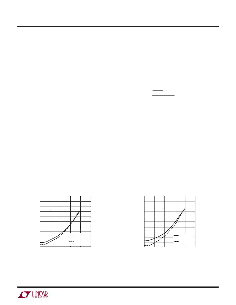
�Thermal� Considerations� and� Output� Current� Derating�
�The� power� loss� curves� in� Figures� 4� and� 5� can� be� used� in�
�coordination� with� the� load� derating� curves� in� Figures� 6�
�through� 13� for� calculating� an� approximate� θ� JA� for� the�
�module� with� and� without� heat� sinking� methods� with� vari-�
�ous� air?ow� conditions.� Thermal� models� are� derived� from�
�several� temperature� measurements� at� the� bench,� and� are�
�correlated� with� thermal� analysis� software.� Tables� 2� and� 3�
�provide� a� summary� of� the� equivalent� θ� JA� for� the� noted�
�conditions.� These� equivalent� θ� JA� parameters� are� correlated�
�to� the� measured� values� and� improve� with� air� ?ow.� The�
�maximum� junction� temperature� is� monitored� while� the�
�derating� curves� are� derived.�
�2.0�
�1.8�
�1.6�
�1.4�
�1.2�
�1.0�
�0.8�
�0.6�
�0.4�
�5V� TO� 1.2V�
�POWER� LOSS�
�0.4�
�5V� TO� 2.5V�
�POWER� LOSS�
�0.2�
�0�
�0�
�1�
�2�
�3�
�3.3V� TO� 1.2V�
�POWER� LOSS�
�4�
�5�
�0.2�
�0�
�0�
�1�
�2� 3�
�3.3V� TO� 2.5V�
�POWER� LOSS�
�4�
�5�
�LOAD� CURRENT� (A)�
�4604� F04�
�Figure� 4.� 1.2V� Power� Loss�
�LOAD� CURRENT� (A)�
�4604� F05�
�Figure� 5.� 2.5V� Power� Loss�
�4604fa�
�11�
�发布紧急采购,3分钟左右您将得到回复。
相关PDF资料
LTM4605EV#PBF
IC DC/DC UMODULE 5A 141-LGA
LTM4606MPV#PBF
IC DC/DC UMODULE 6A 133-LGA
LTM4607IV#PBF
IC BUCK/BOOST SYNC ADJ 5A 141LGA
LTM4608AEV#PBF
IC BUCK SYNC ADJ 8A 68LGA
LTM4608IV#PBF
IC DC/DC UMODULE 8A 68-LGA
LTM4609IV#PBF
IC BUCK/BOOST SYNC ADJ 4A 141LGA
LTM4612IV#PBF
IC BUCK SYNC ADJ 5A 133LGA
LTM4613MPV#PBF
IC UMODULE DC/DC 8A 133-LGA
相关代理商/技术参数
LTM4604IV#PBF
制造商:Linear Technology 功能描述:IC SWITCH MODE DC/DC POWER SUPPLY LGA-66
LTM4604IVPBF
制造商:Linear Technology 功能描述:Conv DC-DC Single-Out Step Down
LTM4604IV-PBF
制造商:LINER 制造商全称:Linear Technology 功能描述:Low Voltage, 4A DC/DC μModuleTM with Tracking
LTM4604V
制造商:LINER 制造商全称:Linear Technology 功能描述:Low Voltage, 4A DC/DC μModuleTM with Tracking
LTM4605
制造商:LINER 制造商全称:Linear Technology 功能描述:High Effi ciency Buck-Boost DC/DC μModule
LTM4605EV#PBF
功能描述:IC DC/DC UMODULE 5A 141-LGA RoHS:是 类别:电源 - 板载 >> DC DC Converters 系列:µModule® 设计资源:VI-200, VI-J00 Design Guide, Appl Manual 标准包装:1 系列:* 类型:隔离 输出数:1 电压 - 输入(最小):66V 电压 - 输入(最大):160V Voltage - Output 1:12V Voltage - Output 2:- Voltage - Output 3:- 电流 - 输出(最大):* 电源(瓦) - 制造商系列:50W 电压 - 隔离:* 特点:* 安装类型:通孔 封装/外壳:9-FinMod 尺寸/尺寸:4.60" L x 1.86" W x 0.79" H(116.8mm x 47.2mm x 20.1mm) 包装:散装 工作温度:-25°C ~ 85°C 效率:* 电源(瓦特)- 最大:*
LTM4605EV#PBF
制造商:Linear Technology 功能描述:IC SMPS CONTROLLER CURRENT-MODE LGA
LTM4605EVPBF
制造商:Linear Technology 功能描述:Conv DC-DC Step Up Step Down